Products

Chip Probing


Chip Probing is to needle test each grain on the wafer, and the probe is equipped with gold wire made of gold wire on the detection head, and the contact (pad) on the grain is in contact to test its electrical characteristics, and the unqualified grain will be marked, and then when the wafer is cut into independent grains according to the grain unit, the unqualified grain marked will be eliminated and no longer proceed to the next process, so as not to increase the manufacturing cost. After wafer fabrication is complete, Chip Probing is a very important step in testing. This step of testing is a transcript of the wafer production process. During the test, the electrical ability and circuit function of each chip are detected. Chip Probing is also known as die sort or wafer sort.
Contact us

Hotline:0771-2568999

Product details

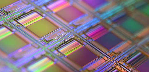
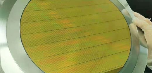
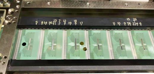
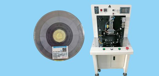
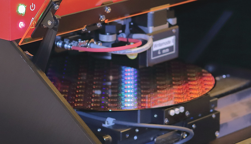
CP testing sits between wafer fabrication and packaging throughout the chip fabrication process. The test object is for each die in the entire wafer, and the purpose is to ensure that each die in the wafer basically meets the characteristics or design specifications of the device, usually including verification of voltage, current, timing, and functionality.

晶圆测试

6f4a47705882c917

晶圆测试2


×
添加微信好友,了解更多产品

点击复制微信号

微信号:

复制成功
微信号:
添加微信好友,了解更多产品
去微信添加好友吧

Tel

0771-2568999

TOP